OEM7720 interface connector
P1901 main connector 60-pin socket
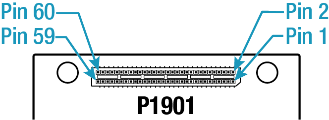
For information about the recommended mating connector, refer to Table: OEM7 communication and I/O connectors.
|
Pin |
Signal name |
Signal type |
Signal direction |
VIL max (V) |
VIH min (V) |
VOL max (V) |
VOH min (V) |
Drive (mA) |
Description |
|
1 |
3V3 |
Power |
Input |
- |
- |
- |
- |
- |
3.2 to 5.0 V ±5% supply input |
|
2 |
3V3 |
Power |
Input |
- |
- |
- |
- |
- |
3.2 to 5.0 V ±5% supply input |
|
3 |
COM2_TXD |
3.3V CMOS |
Output |
- |
- |
0.2 |
3.1 |
4 |
COM2 Transmit Data (UART) |
|
4 |
COM1_TXD |
3.3V CMOS |
Output |
- |
- |
0.55 |
2.3 |
24 |
COM1 Transmit Data (UART) |
|
5 |
COM5_TXD/ COM2_RTS |
3.3V CMOS |
Output |
- |
- |
0.2 |
3.1 |
4 |
This pin is internally multiplexed. COM5_TXD: COM5 Transmit Data (UART). COM2_RTS: COM2 Request to Send |
|
6 |
COM1_RTS |
3.3V CMOS |
Output |
- |
- |
0.2 |
3.1 |
4 |
COM1 Request to Send |
|
7 |
GND |
Ground |
- |
- |
- |
- |
- |
- |
Ground reference |
|
8 |
GND |
Ground |
- |
- |
- |
- |
- |
- |
Ground reference |
|
9 |
COM2_RXD |
3.3V CMOS |
Input |
0.8 |
1.7 |
- |
- |
- |
COM2 Receive Data (UART) |
|
10 |
COM1_RXD |
3.3V CMOS |
Input |
0.8 |
1.7 |
- |
- |
- |
COM1 Receive Data (UART) |
|
11 |
COM5_RXD/ COM2_CTS |
3.3V CMOS |
Input |
0.8 |
1.7 |
- |
- |
- |
This pin is internally multiplexed. COM5_RXD: COM5 Receive Data (UART). COM2_CTS: COM2 Clear to Send |
|
12 |
COM1_CTS |
3.3V CMOS |
Input |
0.8 |
1.7 |
- |
- |
- |
COM1 Clear To Send |
|
13 |
COM4_RXD |
3.3V CMOS |
Input |
0.8 |
1.7 |
- |
- |
- |
COM4 Receive Data (UART) |
|
14 |
COM3_RXD |
3.3V CMOS |
Input |
0.8 |
1.7 |
- |
- |
- |
COM3 Receive Data (UART) |
|
15 |
STATUS_GREEN |
3.3V CMOS |
Output |
- |
- |
0.2 |
3.1 |
4 |
Used to indicate the state of the receiver or provide error codes. These outputs provide the same information as the Status Indicator LED (see Status LED). STATUS_GREEN high and STATUS_RED low represents a Green LED. STATUS_GREEN high and STATUS_RED high represents a Yellow LED. STATUS_GREEN low and STATUS_RED high represents a Red LED. |
|
16 |
STATUS_RED |
3.3V CMOS |
Output |
- |
- |
0.2 |
3.1 |
4 |
|
|
17 |
EVENT_OUT1 |
3.3V CMOS |
Output |
- |
- |
0.2 |
3.1 |
8 |
EVENT1 (Mark1) Output Outputs a user-specified timing signal. Can be synchronized with PPS. Supports Variable Frequency Output function. |
|
18 |
ME_RDY |
3.3V CMOS |
Output |
- |
- |
0.2 |
3.1 |
4 |
Receiver Ready Indicates to the host system that the receiver is ready to receive commands. This signal is not asserted while booting or during a reset. Internal 2.2 kΩ pull down. |
|
19 |
COM4_TXD |
3.3V CMOS |
Output |
- |
- |
0.2 |
3.1 |
4 |
COM4 Transmit Data (UART) |
|
20 |
COM3_TXD |
3.3V CMOS |
Output |
- |
- |
0.2 |
3.1 |
4 |
COM3 Transmit Data (UART) |
|
21 |
ERROR |
3.3V CMOS |
Output |
- |
- |
0.2 |
3.1 |
4 |
Error Indicator Normally low. A high output on this pin indicates that the receiver is in an error state. Internal 2.2 kΩ pull down. |
|
22 |
POS_VALID |
3.3V CMOS |
Output |
- |
- |
0.2 |
3.1 |
4 |
Position Valid Output A high output on this pin indicates that the receiver has computed a valid GNSS position. Internal 10 kΩ pull down. |
|
23 |
EVENT_OUT3 |
3.3V CMOS |
Output |
- |
- |
0.2 |
3.1 |
8 |
EVENT3 (Mark3) Output Outputs a user-specified timing signal. Can be synchronized with PPS. Supports Variable Frequency Output function. |
|
24 |
PPS |
3.3V CMOS |
Output |
- |
- |
0.55 |
2.3 |
24 |
Pulse Per Second output This signal defaults to one pulse per second but may be altered across a wide range of frequencies using software commands. Edges can be synchronized to GNSS time reference. |
|
25 |
EVENT_OUT4 |
3.3V CMOS |
Output |
- |
- |
0.2 |
3.1 |
8 |
EVENT4 (Mark4) Output Outputs a user-specified timing signal. Can be synchronized with PPS. Supports Variable Frequency Output function. |
|
26 |
EVENT_OUT2 |
3.3V CMOS |
Output |
- |
- |
0.2 |
3.1 |
8 |
EVENT2 (Mark2) Output Outputs a user-specified timing signal. Can be synchronized with PPS. Supports Variable Frequency Output function. |
|
27 |
GND |
Ground |
- |
- |
- |
- |
- |
- |
Ground reference |
|
28 |
GND |
Ground |
- |
- |
- |
- |
- |
- |
Ground reference |
|
29 |
EVENT_IN2 |
3.3V CMOS |
Input |
0.8 |
1.7 |
- |
- |
- |
EVENT2 (Mark2) input Rising or falling edge triggered. This input is used to provide a position or time data log based on an external trigger. Internal 10 kΩ pull up. |
|
30 |
EVENT_IN1 |
3.3V CMOS |
Input |
0.8 |
1.7 |
- |
- |
- |
EVENT1 (Mark1) input Rising or falling edge triggered. This input is used to provide a position or time data log based on an external trigger. Internal 10 kΩ pull up. |
|
31 |
EVENT_IN4 |
3.3V CMOS |
Input |
0.8 |
1.7 |
- |
- |
- |
EVENT4 (Mark4) input Rising or falling edge triggered. This input is used to provide a position or time data log based on an external trigger. Internal 10 kΩ pull up. |
|
32 |
EVENT_IN3 |
3.3V CMOS |
Input |
0.8 |
1.7 |
- |
- |
- |
EVENT3 (Mark3) input Rising or falling edge triggered. This input is used to provide a position or time data log based on an external trigger. Internal 10 kΩ pull up. |
|
33 |
GND |
Ground |
- |
- |
- |
- |
- |
- |
Ground reference |
|
34 |
GND |
Ground |
- |
- |
- |
- |
- |
- |
Ground reference |
|
35 |
CAN2_RXD |
3.3V CMOS |
Input |
0.8 |
1.7 |
- |
- |
- |
CAN2 Receive Data This is a CMOS-level signal, requiring an external CAN transceiver. |
|
36 |
CAN1_TXD |
3.3V CMOS |
Output |
- |
- |
0.2 |
3.1 |
4 |
CAN1 Transmit Data This is a CMOS-level signal, requiring an external CAN transceiver. |
|
37 |
CAN2_TXD |
3.3V CMOS |
Output |
- |
- |
0.2 |
3.1 |
4 |
CAN2 Transmit Data This is a CMOS-level signal, requiring an external CAN transceiver. |
|
38 |
CAN1_RXD |
3.3V CMOS |
Input |
0.8 |
1.7 |
- |
- |
- |
CAN1 Receive Data This is a CMOS-level signal, requiring an external CAN transceiver. |
|
39 |
I2C_SDA |
3.3V CMOS Open drain |
I/O |
0.7 |
2.0 |
0.4 |
2.9 |
- |
I2C data line Open drain signal with internal 2.2 kΩ pull up to 3.3 V |
|
40 |
I2C_SCL |
3.3V CMOS Open drain |
Output |
- |
- |
0.4 |
3.1 |
- |
I2C clock line Open drain signal with internal 2.2 kΩ pull up to 3.3 V |
|
41 |
SPI_MOSI |
3.3V CMOS |
Output |
- |
- |
0.2 |
3.1 |
4 |
Serial Peripheral Interface Master Output/Slave Input |
|
42 |
SPI_nCS |
3.3V CMOS |
Output |
- |
- |
0.2 |
3.1 |
4 |
Serial Peripheral Interface Chip Select |
|
43 |
SPI_MISO |
3.3V CMOS |
Input |
0.8 |
1.7 |
- |
- |
- |
Serial Peripheral Interface Master Input/Slave Output |
|
44 |
SPI_SCLK |
3.3V CMOS |
Output |
- |
- |
0.2 |
3.1 |
4 |
Serial Peripheral Interface Serial Clock |
|
45 |
GND |
Ground |
- |
- |
- |
- |
- |
- |
Ground reference |
|
46 |
GND |
Ground |
- |
- |
- |
- |
- |
- |
Ground reference |
|
47 |
USB1_D- |
Analog |
I/O |
- |
- |
- |
- |
- |
USB1 signal. This is one half of the USB1 differential pair. USB1_D+ and USB1_D- must be length-matched and routed as a 90 Ω differential pair. |
|
48 |
USB0_D+ |
Analog |
I/O |
- |
- |
- |
- |
- |
USB0 signal. This is one half of the USB0 differential pair. USB0_D+ and USB0_D- must be length-matched and routed as a 90 Ω differential pair. |
|
49 |
USB1_D+ |
Analog |
I/O |
- |
- |
- |
- |
- |
USB1 signal. This is one half of the USB1 differential pair. USB1_D+ and USB1_D- must be length-matched and routed as a 90 Ω differential pair. |
|
50 |
USB0_D- |
Analog |
I/O |
- |
- |
- |
- |
- |
USB0 signal. This is one half of the USB0 differential pair. USB0_D+ and USB0_D- must be length-matched and routed as a 90 Ω differential pair. |
|
51 |
UID |
3.3V CMOS |
Input |
- |
- |
- |
- |
- |
USB Port Mode Select. Leave this pin floating to put USB0 into Device mode and USB1 into Host mode. Tie this pin to GND to put USB0 into Host mode and USB1 into Device mode. Internal 10 kΩ pull up |
|
52 |
USB0_VBUS |
Power |
I/O |
3.3 |
5.25 |
- |
- |
- |
When the USB port mode is set to Host, this pin is an output. When the USB port mode is set to Device, this pin is an input. Host or Device mode is set using the USB_Port_Mode_Select pin (Pin 51). When an input, requires a voltage between 3.3 V and 5.25 V. When an output, provides 5 V for hosted devices USB0_VBUS is capable of providing up to 200 mA to a hosted USB device. Devices that require more than 200 mA must be powered separately. |
|
53 |
nRESET_IN |
3.3V CMOS |
Input |
0.8 |
2.55 |
- |
- |
- |
Reset Input Resets the OEM7720 receiver card. This pin must be held low for >20 µs while stable power is already applied, to reset the OEM7720 card. It is recommended to hold the nRESET_IN pin low for a >150 ms when initially applying power to the card, giving the power supply time to stabilize before the card starts to boot. Internal 10 kΩ pullup. |
|
54 |
GND |
Ground |
- |
- |
- |
- |
- |
- |
Ground reference |
|
55 |
ETH_LINK_ACT |
3.3V CMOS |
Output |
- |
- |
0.2 |
3.1 |
8 |
Ethernet Link and Activity LED indicator. Polarity of the indicator signal is low. When there is an active link, the pin is low. When there is activity on the link, the pin outputs a blink signal. Do not use ETH_BIAS to supply the LED. |
|
56 |
ETH_BIAS |
Power |
Output |
- |
- |
- |
- |
- |
DC Bias source for the Ethernet magnetics. Do not use ETH_BIAS to supply any other circuitry. |
|
57 |
ETH_RX+ |
Analog |
Input |
- |
- |
- |
- |
- |
Ethernet Receive One half of the Ethernet receive differential pair. ETH_RX+ and ETH_RX- must be routed as a 100 Ω differential pair. |
|
58 |
ETH_TX+ |
Analog |
Output |
- |
- |
- |
- |
- |
Ethernet Transmit One half of the Ethernet transmit differential pair. ETH_TX+ and ETH_TX- must be routed as a 100 Ω differential pair. |
|
59 |
ETH_RX- |
Analog |
Input |
- |
- |
- |
- |
- |
Ethernet Receive One half of the Ethernet receive differential pair. ETH_RX+ and ETH_RX- must be routed as a 100 Ω differential pair. |
|
60 |
ETH_TX- |
Analog |
Output |
- |
- |
- |
- |
- |
Ethernet Transmit One half of the Ethernet transmit differential pair. ETH_TX+ and ETH_TX- must be routed as a 100 Ω differential pair. |