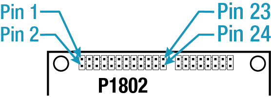
OEM729 interface connectors
P1802 main connector 24-pin header
For information about the recommended mating connector, refer to Table: OEM7 communication and I/O connectors.
|
Pin |
Signal name |
Signal type |
Signal direction |
VIL max (V) |
VIH min (V) |
VOL max (V) |
VOH min (V) |
Drive (mA) |
Description |
|
1 |
GND |
PWR |
- |
- |
- |
- |
- |
- |
Ground reference |
|
2 |
USER11 |
3.3V CMOS |
Input/ |
0.7 |
2.1 |
0.4 |
2.9 |
4 |
User GPIO. Internal 10 kΩ pulldown. |
|
3 |
VARF |
3.3V CMOS |
Output |
- |
- |
0.4 |
2.9 |
4 |
Variable Frequency output Edges can be synchronized to the GNSS time reference. Internal 10 kΩ pullup |
|
4 |
PPS |
3.3V CMOS |
Output |
- |
- |
0.4 |
2.4 |
16 |
Pulse Per Second output This signal defaults to one pulse per second but may be altered across a wide range of frequencies using software commands. Edges can be synchronized to GNSS time reference. |
|
5 |
3V3 |
PWR |
- |
- |
- |
- |
- |
- |
3.3 V ±5% supply input |
|
6 |
3V3 |
PWR |
- |
- |
- |
- |
- |
- |
3.3 V ±5% supply input |
|
7 |
COM3_RX/ |
3.3V CMOS |
Input |
0.7 |
2.1 |
- |
- |
- |
This pin is internally multiplexed. COM3_RX: COM3 receive data input. EVENT2 input. Rising or falling edge triggered. This is used to provide position or time data on an external trigger. Internal 10 kΩ pullup. |
|
8 |
EVENT1 |
3.3V CMOS |
Input |
0.7 |
2.1 |
- |
- |
- |
EVENT1 input Rising or falling edge triggered. This input is used to provide a position or time data log based on an external trigger. Internal 10 kΩ pullup. |
|
9 |
ERROR |
3.3V CMOS |
Output |
- |
- |
0.4 |
2.9 |
4 |
ERROR output Normally low. A high output on this pin indicates that the receiver is in an error state. Internal 10 kΩ pulldown. |
|
10 |
PV |
3.3V CMOS |
Output |
- |
- |
0.4 |
2.9 |
4 |
Position Valid output A high output on this pin indicates that the receiver has computed a valid GNSS position. Internal 10 kΩ pulldown. |
|
11 |
COM2_CTS |
3.3V CMOS |
Input |
0.7 |
2.1 |
- |
- |
- |
COM2 Clear To Send input This is an optional flow control signal for the COM2 UART. Internal weak (40 kΩ to 100 kΩ) pullup. |
|
12 |
nRESET_IN |
Other |
Input |
0.8 |
2.3 |
- |
- |
- |
Active Low. Resets the OEM729 receiver card. This pin must be held low for >20 µs while stable power is already applied, to reset the OEM729 card. It is recommended to hold the nRESET_IN pin low for a >150 ms when initially applying power to the card, giving the power supply time to stabilize before the card starts to boot. Internal 10 kΩ pullup. |
|
13 |
COM2_RTS |
3.3V CMOS |
Output |
- |
- |
0.4 |
2.9 |
4 |
COM2 Request To Send output This is an optional flow control signal for the COM2 UART. |
|
14 |
COM2_RX |
3.3V CMOS |
Input |
0.7 |
2.1 |
- |
- |
- |
COM2 Receive Data input Internal weak (40 kΩ to 100 kΩ) pullup. |
|
15 |
COM1_CTS/ |
COM1_CTS: RS-232 |
Input |
- |
- |
- |
- |
- |
This pin is internally multiplexed. COM1_CTS is the default. COM1_CTS: COM1 Clear To Send input. This is an optional flow control signal for the COM1 UART (±25V tolerant). COM1_RXD-: This is one half of the COM1 RS-422 receive differential pair (2V differential typical) |
|
COM1_RXD-: RS-422 |
Input |
- |
- |
- |
- |
- |
|||
|
16 |
COM2_TX |
3.3V CMOS |
Output |
- |
- |
0.4 |
2.9 |
4 |
COM2 Transmit Data output |
|
17 |
COM1_RTS/ COM1_TXD- |
COM1_RTS: |
Output |
- |
- |
- |
- |
- |
This pin is internally multiplexed. COM1_RTS is the default. COM1_RTS: COM1 Request To Send output. This is an optional flow control signal for the COM1 UART (±25V tolerant). COM1_TXD-: This is one half of the COM1 RS-422 transmit differential pair. (2V differential typical) |
|
COM1_TXD-: |
Output |
- |
- |
- |
- |
- |
|||
|
18 |
COM1_RX/ |
COM1_RX: |
Input |
0.7 |
2.1 |
- |
- |
- |
This pin is internally multiplexed. COM1_RX is the default. COM1_RX: COM1 Receive Data input (±25V tolerant). COM1_RXD+: This is one half of the COM1 RS-422 receive differential pair (2V differential typical). |
|
COM1_RXD+: |
Input |
- |
- |
- |
- |
- |
|||
|
19 |
COM3_TX/USER0 |
3.3V CMOS |
COM3_TX: |
- |
- |
0.4 |
2.9 |
4 |
This pin is internally multiplexed. COM3_TX is the default. COM3_TX: COM3 Transmit Data output. USER0: User GPIO. Internal 10 kΩ pulldown. |
|
USER0: |
0.7 |
2.1 |
- |
- |
- |
||||
|
20 |
COM1_TX/ |
COM1_TX: |
Output |
- |
- |
- |
- |
- |
This pin is internally multiplexed. COM1_TX is the default. COM1_TX: COM1 Transmit Data output. (±25V tolerant) COM1_TXD+: This is one half of the COM1 RS-422 transmit differential pair (2V differential typical) |
|
COM1_TXD+: |
Output |
- |
- |
- |
- |
- |
|||
|
21 |
USB_D- |
Analog |
Input/ |
- |
- |
- |
- |
- |
USB device signal. This is one half of the USB differential pair. USB_D+ and USB_D- must be length-matched and routed as a 90 Ω differential pair. |
|
22 |
USB_D+ |
Analog |
Input/ |
- |
- |
- |
- |
- |
USB device signal. This is one half of the USB differential pair. USB_D+ and USB_D- must be length-matched and routed as a 90 Ω differential pair. |
|
23 |
GND |
PWR |
- |
- |
- |
- |
- |
- |
Ground reference |
|
24 |
GND |
PWR |
- |
- |
- |
- |
- |
- |
Ground reference |
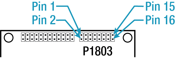
P1803 expansion connector 16-pin header
|
Pin |
Signal name |
Signal type |
Signal direction |
VIL max (V) |
VIH min (V) |
VOL max (V) |
VOH min (V) |
Drive (mA) |
Description |
|
1 |
ETH_RD- |
Analog |
Input |
- |
- |
- |
- |
- |
This is one half of the Ethernet receive differential pair (100 Ω pair). |
|
2 |
ETH_RD+ |
Analog |
Input |
- |
- |
- |
- |
- |
This is one half of the Ethernet receive differential pair (100 Ω pair). |
|
3 |
ETH_BIAS |
PWR |
- |
- |
- |
- |
- |
- |
Centre tap power for Ethernet magnetics. |
|
4 |
ETH_TD+ |
Analog |
Output |
- |
- |
- |
- |
- |
This is one half of the Ethernet transmit differential pair (100 Ω pair). |
|
5 |
ETH_TD- |
Analog |
Output |
- |
- |
- |
- |
- |
This is one half of the Ethernet transmit differential pair (100 Ω pair). |
|
6 |
ETH_BIAS |
PWR |
- |
- |
- |
- |
- |
- |
Centre tap power for Ethernet magnetics. |
|
7 |
LED_A |
3.3V CMOS |
Output |
- |
- |
0.4 |
2.9 |
8 |
Activity/Link indicator output. Polarity of the indicator signal is low. When there is an active link, the pin is low. When there is activity on the link, the pin outputs a blink signal. |
|
8 |
LED_B |
3.3V CMOS |
Output |
- |
- |
0.4 |
2.9 |
8 |
Speed indicator |
|
9 |
GND |
PWR |
- |
- |
- |
- |
- |
- |
Ground reference |
|
10 |
CAN1TX |
3.3V CMOS |
Output |
- |
- |
- |
- |
- |
CAN1 Transmit data |
|
11 |
CAN1RX |
3.3V CMOS |
Input |
- |
- |
- |
- |
- |
CAN1 Receive data |
|
12 |
CAN2TX |
3.3V CMOS |
Output |
- |
- |
- |
- |
- |
CAN2 Transmit data |
|
13 |
CAN2RX |
3.3V CMOS |
Input |
- |
- |
- |
- |
- |
CAN2 Receive data |
|
14 |
UID |
3.3V CMOS |
Input |
- |
- |
- |
- |
- |
USB Port Mode Leave this pin floating to ensure the USB port is in Device mode. Host mode is not currently supported on the OEM729. Internal 10 kΩ pull up |
|
15 |
VBUS |
PWR |
- |
- |
- |
- |
- |
- |
5V output for hosted USB devices |
|
16 |
GND |
PWR |
- |
- |
- |
- |
- |
- |
Ground reference |