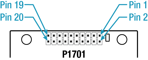
OEM719 interface connector
P1701 main connector 20-pin header

For information about the recommended mating connector, refer to Table: OEM7 communication and I/O connectors.
|
Pin |
Signal name |
Signal type |
Signal direction |
VIL max (V) |
VIH min (V) |
VOL max (V) |
VOH min (V) |
Drive (mA) |
Description |
|
1 |
NC |
- |
- |
- |
- |
- |
- |
- |
No internal connection on OEM719 receiver. (This pin was the supply feed for the external GNSS antenna on the OEM6 family. The OEM719 generates the antenna power from the 3.3V supply input.) |
|
2 |
3V3 |
Power |
- |
- |
- |
- |
- |
- |
3.3 V ±5% supply voltage. This is monitored by the receiver itself. (Out-of-tolerance supply inputs may generate warning or error messages.) |
|
3 |
USB_D- |
Analog |
Input/ |
- |
- |
- |
- |
- |
This is one half of a USB differential pair (pins 3 and 4), match lengths and route as 90 Ω differential pair if USB is used. |
|
4 |
USB_D+/ |
Analog |
USB_D+: |
- |
- |
- |
- |
- |
This pin is internally multiplexed. USB_D+ is the default. USB_D+: This is one half of a USB differential pair (pins 3 and 4), match lengths and route as 90 Ω differential pair if USB is used. RXD3: COM3 Receive Data (UART). Internal weak (40 kΩ to 100 kΩ) pullup. |
|
RXD3 |
0.7 |
2.1 |
- |
- |
- |
||||
|
5 |
nRESET_IN |
3.3V CMOS |
Input |
0.8 |
2.3 |
- |
- |
- |
Active Low. Resets the OEM719 receiver card. This pin must be held low for >20 µs while stable power is already applied, to reset the OEM719 card. It is recommended to hold the nRESET_IN pin low for a >150 ms when initially applying power to the card, giving the power supply time to stabilize before the card starts to boot. Internal 10 kΩ pullup. |
|
6 |
VARF/ |
3.3V CMOS |
VARF: |
- |
- |
0.4 |
2.9 |
4 |
This pin is internally multiplexed. VARF is the default. VARF: Variable Frequency Output. Rising or falling edge active. CAN1RX: a CMOS-level signal, requiring an external CAN transceiver. Internal 10 kΩ pullup. |
|
CAN1RX: |
0.7 |
2.1 |
- |
- |
- |
||||
|
7 |
EVENT2/ |
3.3V CMOS |
EVENT2: |
0.7 |
2.1 |
- |
- |
- |
This pin is internally multiplexed. EVENT2 is the default. EVENT2: Rising edge triggered. CAN1TX is a CMOS-level signal, requiring an external CAN transceiver. Internal 10 kΩ pullup. |
|
CAN1TX: |
- |
- |
0.4 |
2.9 |
4 |
||||
|
8 |
CAN2RX |
3.3V CMOS |
Input |
0.7 |
2.1 |
- |
- |
- |
CAN2RX is a CMOS-level signal, requiring an external CAN transceiver. |
|
9 |
EVENT1/ |
3.3V CMOS |
EVENT1: |
0.7 |
2.1 |
- |
- |
- |
This pin is internally multiplexed. EVENT1 is the default. EVENT1: Rising edge triggered. TXD3: COM3 Transmit Data (UART) Internal 10 kΩ pullup. |
|
TXD3: |
- |
- |
0.4 |
2.9 |
4 |
||||
|
10 |
GND |
Power |
- |
- |
- |
- |
- |
- |
Supply Return (Ground) |
|
11 |
TXD1 |
3.3V CMOS |
Output |
- |
- |
0.8 |
2.0 |
16 |
COM1 Transmit Data (UART) |
|
12 |
RXD1 |
3.3V CMOS |
Input |
0.7 |
2.1 |
- |
- |
- |
COM1 Receive Data (UART) Internal weak (40 kΩ to 100 kΩ) pullup. |
|
13 |
GND |
Power |
- |
- |
- |
- |
- |
- |
Supply Return (Ground) |
|
14 |
TXD2 |
3.3V CMOS |
Output |
- |
- |
0.4 |
2.9 |
4 |
COM2 Transmit Data (UART) |
|
15 |
RXD2 |
3.3V CMOS |
Input |
0.7 |
2.1 |
- |
- |
- |
COM2 Receive Data (UART) Internal weak (40 kΩ to 100 kΩ) pullup. |
|
16 |
GND |
Power |
- |
- |
- |
- |
- |
- |
Supply Return (Ground) |
|
17 |
PV |
3.3V CMOS |
Output |
- |
- |
0.4 |
2.9 |
4 |
Active High. Position Valid Indicator. Indicates that the receiver has computed a position. Active high output. |
|
18 |
GND |
Power |
- |
- |
- |
- |
- |
- |
Supply Return (Ground) |
|
19 |
PPS |
3.3V CMOS |
Output |
- |
- |
0.4 |
2.4 |
16 |
Rising or Falling Edge active. (Software-configurable active edge.) This pin can be configured to provide a GNSS-synchronized time output (commonly Pulse Per Second but can operate at other rates as well). |
|
20 |
CAN2TX |
3.3V CMOS |
Output |
- |
- |
0.4 |
2.9 |
4 |
CAN2TX is a CMOS-level signal, requiring an external CAN transceiver. |