Land pattern and solder stencil design
Note that the module has a large solder pad for thermal mitigation. The pad is tied to Ground.
Recommended PCB pattern (top)
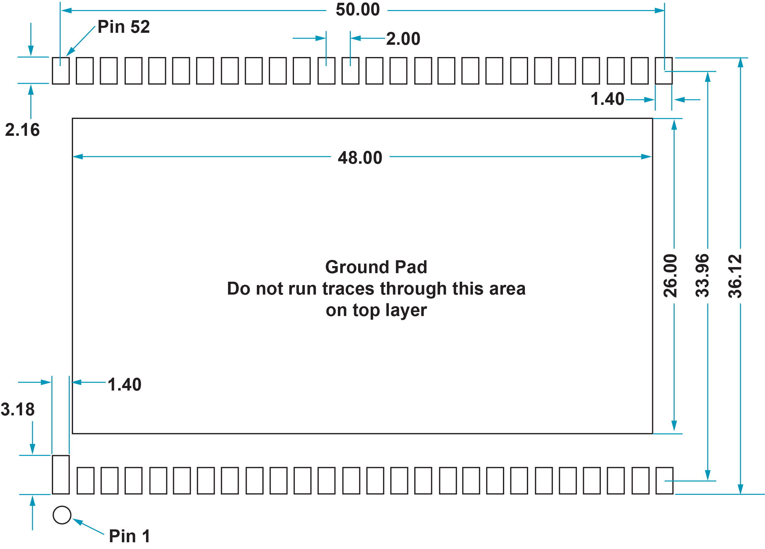
Dimensions are in millimetres
Recommended stencil outline (top)
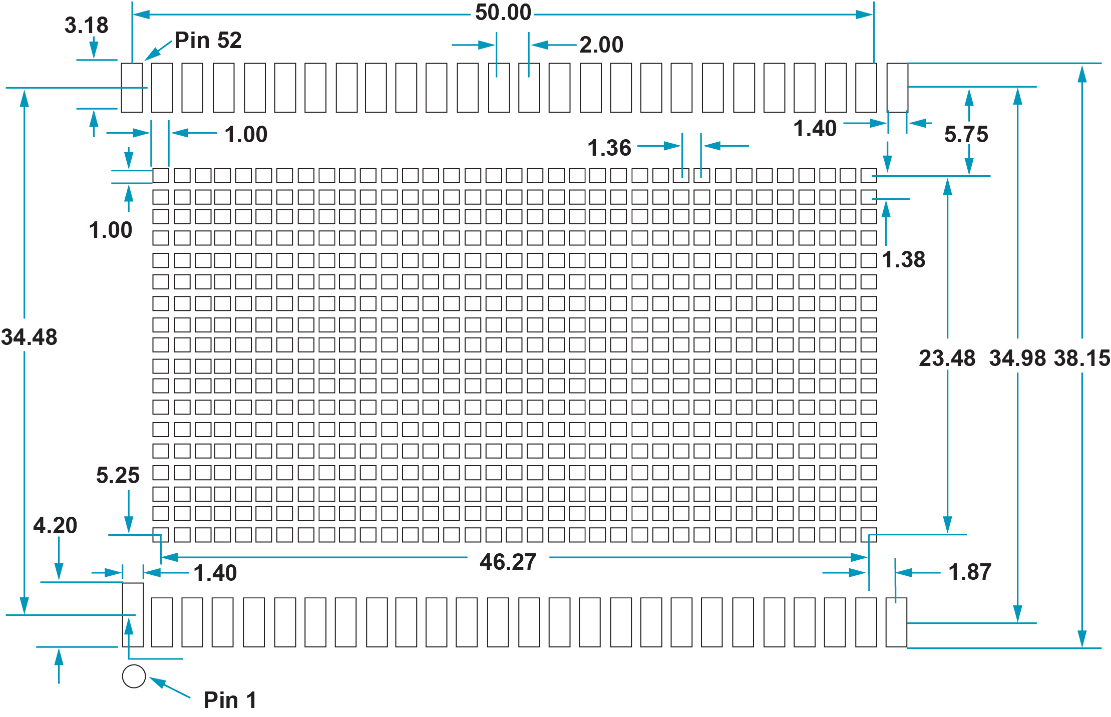
Dimensions are in millimetres
Stencil thickness: 0.127 mm